Vacuum-deposited modification of polymer surfaces

The Oxford invention provides a surface modification method which can be used within a reel-to-reel process under vacuum. The ability to change surface energy allows improvements in film performance in a range of applications. For organic thin film transistors tests have demonstrated a factor of 3-5 times increase in hole mobility at 100% yield.
Film features outstanding performance
Thin polymer films have a broad range of uses which ranges from packaging to electronics, automotive to building materials. Film manufacturers use multiple film layers and surface treatments to control surface energy, wetting, adhesion and a range of other parameters. In the case of creating organic thin film transistors, a particular problem is to modify the dielectric (insulator) layer to ensure that when the semiconductor layer is disposed on top it performs well. Methods of doing this which are “solution-based” are known, but are difficult to use in large scale and at high yield, yet these requirements are fundamental to the attraction of thin film, flexible, electronics! The Oxford invention overcomes this problem by provided a surface modification method which can be used within the required production environment i.e. in a reel-to-reel process under vacuum. The new process offers a number of benefits for film processors:
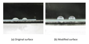
- Demonstrated ability to change surface energy within a high yield production process (images illustrate how processing increases the contact angle from 60° to 90°) this has broad application across a number of fields.
- Improved transistor performance. Tests have demonstrated a factor of 3-5 times increase in hole mobility, e.g. from 0.08cm2/Vs for an untreated sample to 0.44cm2/Vs treated, with a lower threshold swing (1.0V/decade against 1.6V/decade) while maintaining the 100% production yield for these transistors.
- Reduced performance variability within a batch leading to better process capability for example compared to alternative processing techniques e.g. spin-coating.
The Oxford invention was aimed from the outset at high yield, high speed, production processes and although motivated by the challenges of producing organic thin film transistors, the invention has broad application.
Commercial Opportunities
Following successful spin coating trials, the method has been demonstrated on high yield production equipment with the substrate on a moving drum (simulating reel-to-reel behaviour). Funding is being sought to further develop the technique e.g. to understand the range of available materials and optimize processing parameters. This project will be of interest to electronics companies and fast moving consumer goods companies, particularly those working in the field of organic thin film transistors, but also to others working in reel-to-reel film processing e.g. film converters and packaging manufacturers.
about this technology

