Rapid production of large graphene
Making large areas of high quality 2D-materials
A major barrier to the adoption and development of graphene for many promising applications is the lack of graphene available in large sheets of repeatable and uniformally good quality. This invention permits the manufacture of such commercial scale graphene sheets using a transition metal substrate combined with an intermediate silicon containing liquid film.
Current drawbacks
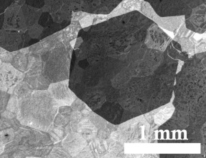
Graphene (and other 2D-materials) grown on solid polycrystalline metals consist of small, irregular domain sizes with many high-angle grain boundaries. This degrades the properties of graphene on the underlying substrate. To improve the quality of the material, the substrate is subjected to post-processing methods that are costly in time and energy such as annealing, mechanical, chemical and electrochemical polishing. Such post-processing will increase the substrate grain size, remove grain boundaries (topographic valleys) and smooth the surfaces. An alternatively expensive solution is to use single crystal substrates of limited size but this is not up-scalable. Additionally, syntheses times on the order of many hours or days are needed for the higher quality materials.
A Practical solution
A method is now available from Oxford Materials Department which overcomes the current problems still using CVD-synthesis processing. High-quality graphene is grown on a liquid metal silicide layer that is formed in situ during CVD-synthesis by reacting the deposited silicon-containing film and the transition metal substrate. When processed in the CVD furnace, the liquid layer will fill in the topographic defects of the substrate; remove the dependence of the material growth on the crystallographic orientation of the substrate (Pt, Pd or another metalic foil) and improve the crystallinity of the 2D-material. Large high quality Graphene flakes which cross hundreds of substrate grains, their boundaries and topographic defects, can then be produced. In addition to the high quality material produced with this method, the syntheses times are reduced by 50 times allowing significant saving in consumables, energy and time.
Readiness for market
The Oxford Invention is the subject of a UK patent application. Further refinements and development of the technology is continuing under a number of applied research programmes with the aim to achieve wafer-sized, transfer-free graphene crystals.
Material samples are available for testing. We are looking for commercial partners to develop a commercial opportunity.
about this technology